PRODUCTS
Conductive tape
Electrostatic chuck tape (ESC tape)
For CVD, sputtering, and plasma etching processes
This is a conductive adhesive tape used to hold wafers on an electrostatic chuck in semiconductor manufacturing processes (CVD, sputtering, and plasma etching). By using this tape, glass wafers, support glass wafers, and insulating MEMS wafers, which previously required the application of a high voltage for the wafers to stick to the electrostatic chuck, can now be held by applying a low voltage. This reduces the stress put on wafers by applying a voltage.
Features
- Conductive tape that can be used in CVD, sputtering, and plasma etching processes.
- Glass wafers and insulating MEMS wafers can be held on an electrostatic chuck by applying a low voltage.
- The base material has excellent plasma resistance.
- The base material and adhesive have heat resistance.
Specification
- Model number:
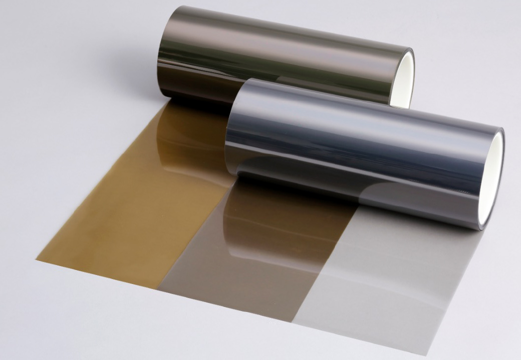
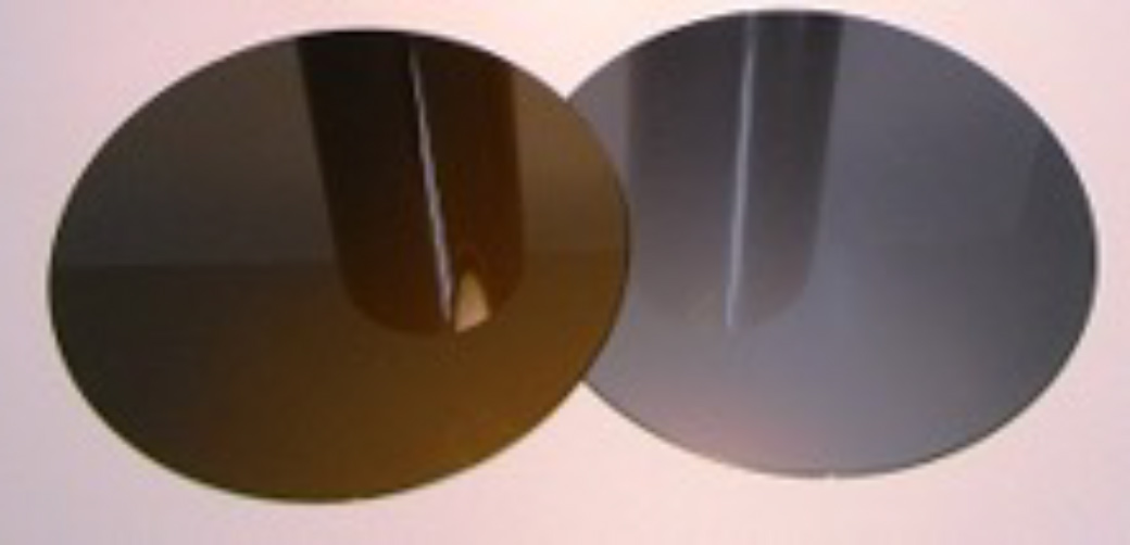
- ①STSI-PEN#25 ②STSI-PI#25
- Material:
- ①Conductive PEN ② Conductive PI
- Width:
- 240±2mm (For φ200mm) or 330±2mm (For φ300mm)
- Length:
- 20m or 80m
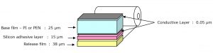
- Base Film Thickness:
- 25±2μm
- Total Thickness:
- 40±4μm
*The film thickness can be changed.
Configuration image
Physical property
| Unit | STSI-PEN#25 | STSI-PI#25 | Measurement | |
|---|---|---|---|---|
| Surface resistivity | Ω/□ | 1.3×10⁵ | 1.3×10⁵ | High resistivity meter |
| Surface resistivity (Adhesive site) |
Ω/□ | >1.3×10¹³ | >1.3×10¹³ | High resistivity meter |
| Decay time | sec | <0.3 | <0.3 | FTM 101C-4046 (23℃×15%RH) |
|
Adhesive strength (vs Glass) |
N/25mm | 0.2 | 0.2 | Peeling Speed : 300mm/min Peeling Angle : 170° |
| Outgassing | μg/g | 34 | 43 | 170℃ 10min. |
| Transparency rate | % | 75 | 47 | JIS K 7105 |
*This data is an actual measurement value, not a guaranteed value.
